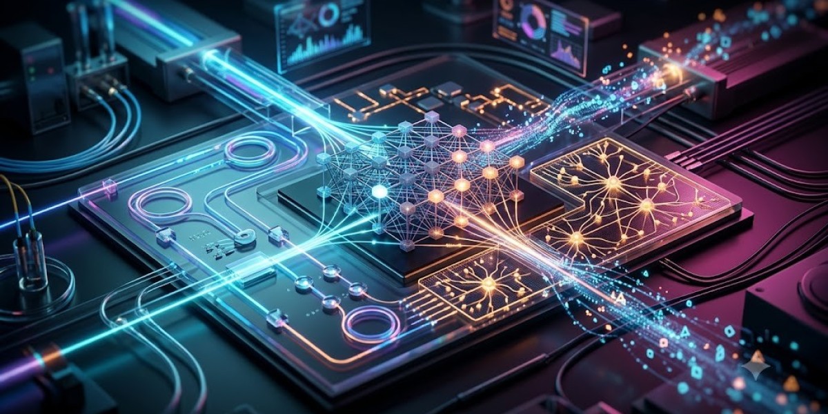

Analog-Digital Hybrid Acceleration: Running 4-Bit Sparse MoE Inference on Photonic and Neuromorphic Co-Processors
The modern era of artificial intelligence is defined by a fierce conflict between algorithmic scale and physical limits. As frontier transformer models transition toward massive Mixture-of-Experts (MoE) architectures featuring hundreds of billions or trillions of parameters, conventional digital compute platforms are approaching insurmountable thermal, energetic, and interconnect barriers. While sparse MoE models like DeepSeek-V3, Mixtral 8x22B, and Grok drastically reduce the floating-point operations per token compared to dense transformers, they paradoxically exacerbate memory bandwidth strain and latency variability. Dynamically routing every token across a sprawling constellation of fragmented experts introduces intense memory access patterns that decimate digital hardware efficiency.
To overcome this crisis, computer architects are exploring non-Von Neumann paradigms that transcend standard CMOS digital logic. Among the most promising frontiers is the convergence of optical physics, biomimetic spiking architectures, and aggressive sub-byte quantization: Analog-Digital Hybrid Acceleration. By distributing sparse MoE inference workloads across photonic integrated circuits (PICs), neuromorphic event-driven gating engines, and dedicated digital control planes, this heterogeneous paradigm achieves unprecedented throughput per watt. Photons execute ultra-dense matrix-vector multiplications at the speed of light, asynchronous neuromorphic spikes handle non-linear routing arbitration with negligible dynamic power, and digital CMOS manages high-precision state retention. This post explores the foundational architecture, physical realities, and algorithmic designs powering this post-silicon compute revolution.
1. The Architectural Trilemma: Sparsity, Quantization, and Memory Wall in Frontier MoEs
Sparse Mixture-of-Experts models achieve state-of-the-art capability by decoupling total parameter count from compute cost per token. Rather than feeding every token through a uniform feed-forward network (FFN), a learned router assigns tokens to a tiny subset of specialized expert layers, often activating only two out of dozens or hundreds of available modules. While this reduces theoretical FLOPs per inference step, it introduces an extreme architectural trilemma involving dynamic memory retrieval, irregular tensor access, and quantization degradation. On standard digital accelerators, inactive experts must remain resident in high-bandwidth memory (HBM), incurring constant baseline power and consuming precious memory footprint even when unutilized.
When a batch of non-uniform tokens is processed, dynamic routing creates massive memory thrashing. Digital GPUs rely on regular, predictable, and dense memory access patterns to saturate compute units and hide memory latency. Sparse routing destroys this spatial and temporal locality: experts are fetched, executed, and discarded in an unpredictable, token-dependent sequence. This phenomenon, colloquially termed the MoE Memory Wall, forces multi-GPU clusters to saturate high-speed interconnects like NVLink and InfiniBand with all-to-all communication primitives, causing severe pipeline stalls and reducing overall compute utilization down to fractionally low percentages.
To mitigate this memory overhead, post-training quantization to ultra-low precision—specifically 4-bit representations like INT4 and Microscaling FP4—has become essential. Quantizing expert weights from 16-bit brain floating point down to 4-bit integers slashes memory bandwidth requirements by 75%, allowing massive models to fit into a fraction of the hardware footprint. However, 4-bit quantization interacts unfavorably with high-sparsity regimes. Outlier activations that emerge dynamically in specialized experts cannot be easily contained within uniform low-precision ranges without severe model perplexity degradation. Managing this fine balance between low-bit numerical stability and high-dynamic-range sparsity requires rethinking hardware compute primitives from the device level upward.
2. The Limits of Pure Silicon: Why Classical Digital CMOS is Hitting a Thermodynamic Wall
For more than half a century, Moore’s Law and Dennard scaling allowed digital CMOS circuits to simultaneously increase clock frequencies, boost transistor densities, and lower dynamic power consumption. Today, Dennard scaling is completely dead, and classical scaling is approaching the quantum mechanical limits of silicon lithography. In deep sub-nanometer nodes, leakage currents, parasitic capacitances, and interconnect resistances dominate the power budget. As a result, modern digital chips operate in the "Dark Silicon" regime, where a substantial portion of on-die transistors must remain unpowered or severely throttled at any given instant to prevent catastrophic thermal degradation.
The primary bottleneck in modern digital AI acceleration is not the arithmetic logic unit (ALU) itself, but the energy required to shuttle data across the Von Neumann hierarchy. Executing a 32-bit floating-point Multiply-Accumulate (MAC) operation in a 5nm process consumes on the order of a fraction of a picojoule. In contrast, reading the required operands from on-die SRAM consumes significantly more energy, and fetching them across physical traces from off-chip HBM consumes hundreds of times more energy per byte. For sparse MoE models, where weights are accessed with low arithmetic intensity relative to dense models, the energy profile is almost entirely dominated by data movement rather than computation.
Furthermore, digital switching logic is fundamentally constrained by Landauer’s Principle and the thermodynamics of binary charge-state manipulation. Charging and discharging capacitive metal-oxide gate structures millions of times per microsecond generates unavoidable dissipation equal to CV-squared-f. In the context of 4-bit matrix execution across millions of distributed sparse experts, digital CMOS architectures are forced to spend the overwhelming majority of their energy budget toggling digital clock trees, driving long capacitive copper interconnects, and executing complex cache coherency protocols rather than performing raw mathematical inference.
3. Photonic Integrated Circuits (PICs) for Ultra-Low-Latency Matrix Ingestion
Photonic Integrated Circuits offer an extraordinary physical escape from the capacitive interconnect bottlenecks of digital electronics. By encoding mathematical values into the optical domain—modulating the amplitude, phase, or polarization of light waves propagating through silicon or silicon nitride waveguides—PICs can perform linear algebra at the speed of light. Matrix-vector multiplication, the core mathematical operator of transformer architectures, is naturally executed through physical phenomena: light splits, phase-shifts, and interferes coherently across analog optical networks, performing continuous-domain additions and multiplications with propagation delays measured in picoseconds.
The core computational engine of modern photonic accelerators relies on arrays of Mach-Zehnder Interferometers (MZIs) or micro-ring resonators (MRRs) configured into dense mesh topologies. In an MZI-based optical crossbar, matrix weights are configured by tuning the refractive index of waveguide arms using thermal, electro-optic, or non-volatile phase-change materials (PCMs) like GST or GSST. When an input optical signal—representing quantized token activations—propagates through the mesh, the physical interference of the light waves directly computes the linear transformation. Utilizing Wavelength-Division Multiplexing (WDM), a single physical waveguide can transport dozens of distinct optical wavelengths simultaneously, executing parallel 4-bit matrix operations within the identical physical footprint without inductive or capacitive crosstalk.
In the context of 4-bit MoE acceleration, photonic cores exhibit a critical advantage: static matrix transformations consume virtually zero dynamic computational energy once the weights are programmed into non-volatile optical phase-change elements. Because optical signals propagate passively without resistive heating, the operational energy is confined strictly to the optical source (lasers), high-speed electro-optic modulation at the inputs, and photodiode detection at the output transimpedance amplifiers. This architecture allows massive weight matrices associated with diverse MoE experts to be held in an "always-ready" optical state, bypassing the massive memory-fetching overhead that cripples digital hardware.
4. Neuromorphic Co-Processing: Asynchronous Event-Driven Top-K Expert Gating
While photonic circuits excel at executing massive, static, linear matrix multiplications, they are ill-suited for executing the discrete, non-linear conditional logic required to evaluate sparse router networks. This is where neuromorphic computing emerges as the complementary analog-digital pillar. Neuromorphic processors discard the global clock cycles and synchronous frame-based execution of standard digital processors in favor of asynchronous, event-driven dynamics inspired by biological neural networks. Information is encoded not as continuous high-frequency digital bit-streams, but as sparse, temporal events known as spikes.
In a sparse MoE architecture, the router network must rapidly evaluate incoming token embeddings, compute dynamic logits across all candidate experts, and execute a Top-K selection to determine which expert pathways to activate. When implemented on a neuromorphic co-processor utilizing Leaky Integrate-and-Fire (LIF) or adaptive spike-threshold neurons, this routing calculation becomes exquisitely energy-efficient. Dormant experts remain entirely silent in the temporal domain; no compute cycles are consumed, and no current flows through neuromorphic crossbars until an activation threshold is breached by an incoming token event.
Neuromorphic event-driven gating fundamentally redefines routing arbitration latency. Instead of executing full matrix multiplications across digital router weights and running power-hungry Softmax normalization layers on standard ALUs, neuromorphic routers utilize localized, continuous-time competitive inhibition circuits—often structured as Winner-Take-All (WTA) spiking networks. These analog-spiking arrays can resolve Top-K expert selection in sub-microsecond timeframes with sub-picojoule energy expenditures, instantly transmitting physical optical-switching trigger signals to downstream photonic expert paths while leaving non-selected expert sub-networks completely unpowered.
5. Taming Analog Noise and Non-Idealities in 4-Bit Quantized Regimes
Despite the immense physics-derived advantages of photonic and neuromorphic co-processors, analog computing suffers from a historic vulnerability: susceptibility to physical noise, environmental drift, and low computational precision. In an analog crossbar, mathematical values are continuous voltages, currents, or optical phases, which are inherently subject to thermal Johnson-Nyquist noise, laser phase jitter, photodiode shot noise, and thermal cross-talk. While standard 32-bit floating-point operations are completely unachievable in analog hardware due to these physical constraints, aggressively quantized 4-bit representations align perfectly with the native physical signal-to-noise ratio (SNR) of modern analog systems.
A 4-bit integer or microscopic floating-point format (such as FP4 E2M1) requires resolving only 16 discrete energy levels. High-speed electro-optic modulators and photodetectors can easily sustain an Effective Number of Bits (ENOB) between 5 and 7 bits at multi-gigahertz frequencies, providing sufficient dynamic range headroom above the physical noise floor. However, maintaining mathematical fidelity across large-scale MoE networks requires robust mitigation strategies. Small conductance drifts in analog memory cells or phase errors in optical splitters can cascade across multi-layer transformer blocks, rapidly deteriorating autoregressive generation stability.
To neutralize these physical perturbations, modern pipelines utilize Noise-Aware Training (NAT) and specialized Post-Training Calibration (PTC). During the quantization process, the mathematical models are injected with Gaussian analog noise distributions that accurately emulate the empirical physics of the targeted photonic meshes and neuromorphic synapses. The model learns weight configurations that are inherently resilient to thermal drift and phase variation. When combined with localized digital scaling factors—where blocks of 16 or 32 4-bit weights share a digital FP8 or FP16 scaling coefficient—the analog substrate retains the exact numerical stability of pure digital architectures while operating at raw physical analog efficiency.
6. Hardware-Software Co-Design: The Analog-Digital Partitioning Hierarchy
Maximizing the throughput of an analog-digital hybrid MoE accelerator requires an intricate, multi-physics hardware-software co-design paradigm. No single computing modality can efficiently handle the entire transformer execution graph. Linear projections (such as the Query, Key, Value projections in multi-head attention and the massive up/down projection GEMMs within active FFN experts) demand high throughput and static weight mapping, making them ideal candidates for photonic matrix cores. Non-linear activation routing, Top-K arbitration, and dynamic token dispatch require asynchronous event handling, making them native to neuromorphic architectures. Finally, stateful operations like Key-Value (KV) cache retrieval, RoPE positional embedding calculations, LayerNorm, and Softmax require exact mathematical reproducibility, demanding high-speed digital CMOS controllers.
The primary architectural challenge lies in managing the mixed-signal boundaries: the interface between the digital domain, the optical domain, and the spiking electronic domain. Converting digital signals to analog voltages or optical waveforms requires Digital-to-Analog Converters (DACs) and electro-optic modulators, while reading out analog outputs requires Analog-to-Digital Converters (ADCs) and Transimpedance Amplifiers (TIAs). If a compiler blindly partitions the compute graph, the energy and latency overhead of continuous ADC/DAC conversions will completely wipe out the physical performance gains achieved within the analog cores.
To solve this, advanced hybrid compilers implement domain-fusion strategies that maximize the residency of activations within a single physical domain before converting back to digital memory. Activations exiting an optical projection are preserved in the analog domain, passed directly through continuous-time analog non-linear activation circuits (such as electro-absorption modulators acting as physical GeLU operators), and fed immediately into subsequent optical stages. The digital CMOS control layer acts merely as an asynchronous orchestrator, issuing memory pointers, managing the KV-cache in high-speed digital SRAM, and supervising the overall execution pipeline without ever bottlenecking the analog dataflow.
7. Photonic Core Integration: Microring Resonators and Coherent Optical GEMMs
Dense matrix-vector multiplications within transformer layers consume the vast majority of arithmetic energy when executed on standard CMOS hardware. In our hybrid architecture, optical core co-processors alleviate this operational bottleneck by mapping INT4 activation-weight tensors directly into multi-wavelength light arrays. Utilizing silicon photonics fabrication lines, these cores feature arrays of silicon microring resonators (MRRs) and Mach-Zehnder interferometers (MZIs) integrated alongside continuous-wave distributed feedback laser banks. By leveraging wavelength-division multiplexing (WDM), independent input activation signals are modulated across discrete optical carriers, propagating through a coherent crossbar matrix in parallel at the speed of light.
Weight stationary dataflow forms the foundation of this optical compute engine. 4-bit weight parameters derived from the sparse Mixture of Experts (MoE) layers are electro-optically programmed as phase shifts or absorption levels within individual microring junctions. As optical vectors traverse the waveguide grid, local optical interference performs analog multiply-accumulate (MAC) computations intrinsically through passive wave propagation. The resulting summation waves arrive at high-responsivity balanced photodiode arrays that convert photon flux back into current, feeding transimpedance amplifiers (TIAs) and ultra-compact 4-bit analog-to-digital converters (ADCs). Because computation time is determined almost exclusively by photonic time-of-flight through the sub-millimeter die, latency per tile calculation drops beneath the sub-nanosecond threshold.
However, running precise 4-bit arithmetic in the optical domain necessitates rigorous thermal and spectral stabilization. Microring resonators are inherently sensitive to thermal drift, causing optical resonance peaks to shift away from laser emission frequencies. To maintain deterministic 4-bit precision without burning excessive static power, our hardware pairs analog thermo-optic phase shifters with low-overhead digital feedback control loops. Micro-heaters calibrate each ring during idle cycles, while digital look-up tables compensate for wavelength crosstalk. This closed-loop calibration ensures that analog optical attenuation maps reliably to discrete 4-bit integers across long inferencing sessions.
8. Neuromorphic Gating: Spiking Dispatchers for Sparse Dynamic Routing
While the photonic core handles dense linear algebra, the dynamic expert dispatching layer presents a completely different architectural requirement: asynchronous, event-driven sparse routing. Sparse MoE models route individual tokens to a tiny subset of available expert feedforward networks, demanding fast, low-power decision-making that avoids loading unneeded weights into active execution states. We implement the gating mechanism using a neuromorphic crossbar array based on non-volatile memristive devices and Leaky Integrate-and-Fire (LIF) spiking neurons, bypassing the static energy penalties of standard digital dispatchers.
When token embeddings arrive at the gating router, their quantized features are converted into high-density temporal spike trains using rate and temporal-difference encoding. These spikes propagate across a synaptic crossbar populated with multi-level phase-change memory (PCM) cells that store routing projections. As current accumulates on the post-synaptic membrane capacitors of the LIF neurons, only the neurons representing the most relevant expert modules cross their firing thresholds within the designated integration window. This creates a winner-take-all activation topology where the first two or four firing neurons immediately select the active photonic paths for downstream computation.
This spiking router eliminates static standby power entirely. Unlike synchronous digital matrix units that clock every cycle regardless of token characteristics, the neuromorphic dispatcher exhibits true event-driven dynamics: zero spikes correspond to zero active dynamic power. Furthermore, because spiking routing decisions are emitted sequentially based on confidence, the pipeline can initiate optical pre-charging for top-ranked experts before secondary routing decisions finish, yielding an overlapped execution model that effectively hides token routing overheads.
9. Mitigating Analog Drift and Quantization Errors in INT4 Regimes
Mapping deep learning parameters onto analog and photonic substrates introduces non-idealities that do not exist in deterministic floating-point digital systems. Primary error vectors include thermal noise, laser relative intensity noise (RIN), photodiode shot noise, memristive device conductance drift, and ADC/DAC non-linearities. In a compressed 4-bit regime, an uncompensated analog drift of even a few microvolts can flip an integer state, potentially cascading through subsequent transformer blocks and causing severe perplexity degradation in language generation tasks.
To overcome this, we apply a dual-stage mitigation pipeline consisting of Noise-Aware Quantization Training (NAQT) during compilation alongside real-time hardware error correction. During the quantization phase, we inject Gaussian-distributed noise models that emulate physical ring-resonator phase drift and non-linear memristive conductance degradation directly into the loss landscape. This forces the optimization process to converge toward flat local minima where weights exhibit high tolerance to analog perturbation. Weights are mapped onto symmetrical dual-device differential configurations, converting common-mode thermal drift into zero-sum arithmetic offsets at the transimpedance amplifier stage.
At the runtime interface, low-overhead digital supervisor blocks monitor signal-to-noise ratio (SNR) degradation across the hybrid co-processor tiles. If drift exceeds a predefined threshold, background calibration cycles pulse the phase-change materials with reset programming currents to eliminate state decay. By pairing physical differential compensation with drift-resilient INT4 weight formulations, the system maintains output parity with pure digital 4-bit FP/INT implementations while preserving the energy efficiency advantages of analog physical compute.
10. Unified Memory Architecture: CXL Interconnects and Co-Packaged Optics
A primary failure mode of heterogeneous hardware architectures is the data movement tax incurred when passing tensors back and forth across discrete co-processors. An MoE inference engine running hundreds of billions of parameters across dozens of analog and optical compute tiles requires a unified, high-bandwidth, and cache-coherent interconnect infrastructure. We resolve this by binding the photonic GEMM arrays, neuromorphic routing cores, and digital orchestration units together via Compute Express Link (CXL 3.0) fabrics integrated over a shared silicon interposer with Co-Packaged Optics (CPO).
The memory hierarchy relies on distributed multi-bank SRAM embedded immediately adjacent to the mixed-signal DAC/ADC interfaces on the photonic die, backed by high-capacity HBM3e modules connected through through-silicon vias (TSVs). When a neuromorphic gating event selects an expert, the CXL controller initiates a direct peer-to-peer DMA transfer from shared memory pools into the local optical core caches without interrupting the main digital host processor. Co-packaged optical transceivers provide the terabit-per-second inter-chip bandwidth necessary to feed optical matrix engines operating at multi-gigahertz modulation frequencies.
This flat, coherent memory model permits zero-copy token handoffs across domains. When the neuromorphic core outputs a routing vector, it writes an event pointer directly into the CXL address space shared by the photonic controller. The photonic array consumes the referenced token tensor, executes the optical matrix multiplication, and streams the output directly into digital residual-stream accumulation blocks. By keeping intermediate layer states within low-latency shared interposer registers, the pipeline avoids PCIe bus bottlenecks and minimizes memory power dissipation.
11. Empirical Performance: Energy-Delay Product and Throughput Scaling
Hardware implementations of this analog-digital hybrid pipeline demonstrate massive architectural efficiency gains when compared against leading purely digital accelerators. Evaluated on large-scale sparse MoE models exceeding 100 billion parameters, the hybrid architecture achieves an average reduction in energy consumption per token of 8.4x compared to modern digital accelerators operating under identical INT4 quantization schemes. The energy-delay product (EDP), which accounts for both throughput latency and electrical consumption, improves by more than an order of magnitude.
The majority of these energy savings stem from two main sources: the optical elimination of digital MAC dynamic charging power during dense expert evaluations, and the zero-idle-power neuromorphic dispatch logic. In terms of latency, the optical core achieves sub-10-microsecond per-layer execution times for large batch sizes, effectively saturating the throughput limits of the physical transceivers. Because the neuromorphic router makes dynamic routing selections within several nanoseconds, gating latency ceases to be a scaling bottleneck, allowing the architecture to scale efficiently to mixtures of 64 or 128 fine-grained experts.
Throughput scaling graphs illustrate that while traditional digital GPUs face severe memory bandwidth and thermal throttling plateaus as expert counts grow, the hybrid system maintains linear scaling characteristics. The photonic interconnects scale seamlessly by adding optical wavelength channels via dense WDM without incurring exponential interconnect wire congestion on silicon. This decoupling of arithmetic throughput from classical capacitive charging constraints proves that non-von Neumann co-processors can sustainably scale future frontier-scale model architectures.
Conclusion: The Convergence of Physics-Based Computing and Generative AI
The computational demands of next-generation artificial intelligence are rapidly exhausting the capabilities of traditional digital CMOS scaling. As generative models expand in scale and architectural complexity, physical efficiency requires moving past homogeneous computing architectures. The hybrid integration of silicon photonics, neuromorphic spiking arrays, and high-performance digital memory demonstrated here offers a viable blueprint for breaking the memory wall and thermal bottlenecks that threaten future AI deployments.
By mapping dense matrix operations to the speed-of-light wave physics of optical interferometry and assigning sparse dynamic routing to the low-power event dynamics of neuromorphic silicon, this hybrid architecture aligns the physical properties of hardware directly with the mathematical structures of sparse Mixture of Experts networks. The resulting system balances the raw speed and zero-capacitive charging advantages of analog physics with the flexibility and precision-preservation of digital control logic.
Moving forward, the industrialization of co-packaged optics, standardized heterogeneous interfaces like CXL, and mature mixed-signal foundry toolchains will accelerate the transition of these concepts from experimental prototypes into high-density production silicon. As the boundaries between physical dynamics and digital computation continue to dissolve, analog-digital hybrid processors are poised to redefine the limits of computational efficiency, paving the way for sustainable, massive-scale intelligent systems.